
A = Add.0
B = Add.1
Ci = Add.2
Sum gate abc ao bo co
Cy gate ab ac bc
abc gate A B Ci
ab gate A B
ac gate A Ci
bc gate B Ci
ao gate A ab ac
bo gate B ab bc
co gate Ci ac bc
Add END
GateSim simulates the action of integrated circuit gates as used in sequential circuits like a computer. A power-on reset signal and both phases of square-wave non-overlapping clock are provided, along with a built-in ROM and RAM macro capability. Simulation is normalized to a standardized gate delay, with memory access delays being somewhat longer, depending on the memory size. You can download a zip file with the executable (.exe) program and this documentation.
The execution of the complete circuit network can be selectively traced at periodic intervals set by the user, and showing the signals selected by the user. Every gate in the circuit is fully redefined from its inputs once for each nominal gate delay, but you typically want to watch sequential circuits just before each clock transition introduces the propagation of new signal values. In the TinyMIPS circuit, you can choose one of several trace intervals, respectively for viewing instruction execution at clock rate, or at 10x clock rate to see signal settling delays, or at gate delay rate to see every excruciating detail.
A macro capability allows the user to define larger components from atomic gates and/or other macros, and then use them by name. Several macros are built-in.
Many of the parts involve a sequence of essentially similar inputs and outputs, such as the bits of an address or data word. GateSim typically numbers these inputs and outputs in numerical order beginning with zero, except that memory addresses are numbered in the reverse order so that they read like normal numbers. We call this "Big-Endian" because we start the numbering at the big end, but unlike conventional Big-Endian schemes, we still number the address and data bits by their powers of two. The data bits and all other sequences in GateSim are true "Little-Endian" because they start the numbering at the little end. See the example for RAM, below.
RunTime -- This is the number of gate delays (or clocks) the simulation runs for each click on the Run button.
ClockRate -- This is the number of gate delays in each phase of the system clock. Failure to choose a delay value large enough to allow all signals to settle before the clock transitions again may result in unpredictable behavior. A very large number here makes the simulation (and effective processor speed) very slow.
PowerOnDelay -- This is the number of clock phases that pass before the built-in RESET signal goes high. The user can set this appropriate to whatever settling time is needed.
TraceRate -- This is the number of gate delays between each trace line. If this number is less than the ClockRate, then the trace lines are numbered by gate delay times; otherwise the trace lines are numbered by clocks. The RunTime value is based on the same criterion, either gate delays or clocks.
You may alternatively put a signal name here, and the trace is triggered whenever that signal goes true. You should use a Pulse to generate this signal, and thus ensure it does not stay true too long and retrigger a secondary or spurious trace line.
TraceDelay -- This is an optional number of gate delays before
the first trace line, default 0 if omitted. Use this to adjust the position
of a trace line that comes out only once (or less) per clock cycle, so
to give the signals time to settle. You can also use it to delay past a
large part of the trace log before it begins to trace, for example to do
a very detailed trace near a problem many cycles after the simulation begins.
NodeName -- This is a unique name for the signal produced by this component. You connect inputs of other components to this output by using this name in their input list.
PartType -- This is the name of the built-in component type or user-defined macro.
InputList -- One or more names, as required for this component,
specify the source signal name for each input to this part. You may also
use here one of the predefined signal names, CLK, CLK/, RESET, 0,
or 1 (see below).
RAM -- This defines a Read Access Memory. The first input item is the number of data lines, followed by the address bit inputs, most-significant first, then the write control,then the data bits, bit 0 (least significant) first. The number of memory cells is defined by the number of address lines given. The output data bits are named by the RAM name plus a bit number, separated by a dot. For example:
Regs RAM 4, Addr2, Addr1, Addr0, wr, Data0, Data1, Data2, Data3has 8 4-bit words, and the outputs can be referenced by Regs.0 (least significant) through Regs.3 (most significant). A RAM is limited to 32 data bits and 16 address bits. The number of address bits is determined by counting off the indicated number of data bits from the right end of the specification line, then the write control signal; all the remaining inputs are address lines.
The write control line is low-active and must be stable for two gate-delays after the address has settled (access time) for a reliable write. The data to be read back out will be undefined for the following access time delay after a write or any address line changes:
1-16 locations, 4 gate delaysROM -- This defines a Read-Only Memory or Programmed Logic Array. The first input item is the number of data lines, followed by the address bit inputs, most-significant first. The number of ROM cells is defined by the number of address lines given. Thus if three address lines are specified, the ROM will have 8 data words. The individual data bits are named by the ROM name plus a bit number, separated by a dot. For example:
32-512 locations, 5 gate delays
1024-16384 locations, 8 gate delays
More than 16384, 13 gate delays
thePLA ROM 12, Addr3, Addr2, Addr1, Addr0has 16 12-bit words, and the outputs can be referenced by thePLA.0 (least significant) through thePLA.11 (most significant). You would normally follow this with one or more DATA lines to specify the outputs for each address. A ROM has the same access time as a comparably sized RAM, and is limited to the same number of data and address bits.
DATA -- This defines the initial contents of the previous ROM (or RAM). Instead of a part name, the first item on this line is the address to be loaded, and instead of inputs, the remaining data is the memory values. Values may be in binary, decimal, or hexadecimal. Binary values must specify the full word size in bits, and hexadecimal values must begin with a zero (but be fewer characters than there are bits); decimal values begin with a non-zero digit. It is not possible to give hexadecimal values for a 2-bit word size (but decimal values are the same). The starting address may be hexadecimal (with a leading zero) or decimal (any other digit). The following example loads up the first 12 locations of the previous example ROM with a sliding bit pattern, followied by a four-word checkerboard:
0 DATA 000000000001, 2, 04, 000000001000, 16, 020, 040, 128= -- This defines the name on its left to be the same signal as the name on its right (which must be otherwise defined). You can use this to give more meaningful names to larger component outputs, such as:
8 DATA 256, 0200, 010000000000, 2048
12 DATA 101010101010, 010101010101, 0AAA, 1365
LeastBit = thePLA.0CHIP -- This begins a macro definition. The name in the first item of this line is the new part name being defined. The first item to the right is the number of inputs, followed by the (internal) names of the outputs. When the macro is used, the specified number of inputs will be supplied to the right of the part name; outputs will be named by the name on the invocation line and numbered like the memory references. The following lines are all gates included in the macro, up to the macro END line. The END line must have the same name as its corresponding CHIP line. Here is an example of a full adder macro definition (this part is already included in the built-in macros):
Add CHIP 3 Cy SumIn this example, the three inputs are renamed for internal purposes as A, B, and Ci (carry-in). The outputs are the internal names Cy (carry-out) and Sum, which will be respectively numbered FullAdd.0 and FullAdd.1 by the following invocation:
A = Add.0
B = Add.1
Ci = Add.2
Sum gate abc ao bo co
Cy gate ab ac bc
abc gate A B Ci
ab gate A B
ac gate A Ci
bc gate B Ci
ao gate A ab ac
bo gate B ab bc
co gate Ci ac bc
Add END
FullAdd Add Ain, Bin, CinHEX -- This is used to specify trace information. The (one-word) name to the left is the column header, and the inputs are collected together, four at a time, into hexadecimal data to be traced unter that header. For a binary trace, insert three zeros between each binary item. For example, the following three lines trace the inputs and outputs of the FullAdd line above:
Inputs HEX Ain 0 0 0 Bin 0 0 0 CinNote that if the number of signals to be traced are not a multiple of 4, zeros on the left are assumed. This will produce the following trace:
Sum HEX FullAdd.1
Cy HEX FullAdd.0
Inputs Sum Cy
000 0 0
100 1 0
010 1 0
110 0 1
...
Add -- Full Adder. See description above.
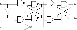 FF
-- Master/Slave Flip-Flop. This implements the circuit in the diagram,
with a data input D, a high-active load control L, and both a Q and Q/
(complement) output. The outputs change on the falling edge of L. NOTE:
this flip-flop will start to oscillate if the inputs change too close to
when the clock fires. For best results, use a properly delayed pulse (see
Pulse
below) for the clock.
FF
-- Master/Slave Flip-Flop. This implements the circuit in the diagram,
with a data input D, a high-active load control L, and both a Q and Q/
(complement) output. The outputs change on the falling edge of L. NOTE:
this flip-flop will start to oscillate if the inputs change too close to
when the clock fires. For best results, use a properly delayed pulse (see
Pulse
below) for the clock.
FF CHIP 2 Q Q/Cnt4 -- 4-Bit Synchronous Counter, as defined by this macro:
D = FF.0
L = FF.1
D/ gate D
L/ gate L
Q gate Q/ mqg
Q/ gate Q nqg
mqg gate L/ mq
nqg gate L/ nq
mq gate nq dg
nq gate mq ndg
dg gate D L
ndg gate D/ L
FF END
Cnt4 CHIP 6 Q0.0 Q1.0 Q2.0 Q3.0The four inputs and first four outputs are the four bits of the counter; the fifth input is a low-active Load control: low loads the inputs into the counter on the clock pulse, and high counts up on the clock. The last input is the clock. Note that this macro makes use of the previous FF macro, which means that the input is captured on the rising edge and the output is updated on the falling edge. Nested macros are permitted, provided that each macro is defined earlier in the source file than its first use. There is no such restriction on the order of gates in the source file.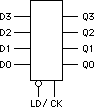
L0 gate Ld Cnt4.0
L1 gate Ld Cnt4.1
L2 gate Ld Cnt4.2
L3 gate Ld Cnt4.3
Q0 FF D0 Cnt4.5
Q1 FF D1 Cnt4.5
Q2 FF D2 Cnt4.5
Q3 FF D3 Cnt4.5
D0 gate c0 L0
D1 gate c1 s1 L1
D2 gate c2 s2 t2 L2
D3 gate c3 s3 t3 u3 L3
c0 gate Q0.1 Cnt4.4
c1 gate Q1.1 Q0.0 Cnt4.4
c2 gate Q2.1 Q0.0 Q1.0 Cnt4.4
c3 gate Q3.1 Q0.0 Q1.0 Q2.0 Cnt4.4
s1 gate Q1.0 Q0.1 Cnt4.4
s2 gate Q2.0 Q1.1 Cnt4.4
s3 gate Q3.0 Q2.1 Cnt4.4
t2 gate Q2.0 Q0.1 Cnt4.4
t3 gate Q3.0 Q1.1 Cnt4.4
u3 gate Q3.0 Q0.1 Cnt4.4
Ld gate Cnt4.4
Cnt4 END
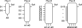
Mux2 -- 4-1 Multiplexor, with two address lines (A0, A1, in that order), to choose from the next four inputs, D0, D1, D2, and D3, thus:
A1 A0 Choose
0 0 D0
0 1 D1
1 0 D2
1 1 D3
Mux3 -- 8-1 Multiplexor. Three address lines and eight data
inputs, A0,A1,A2, D0,D1,D2,D3, D4,D5,D6,D7.
 Mux4
-- 16-1 Multiplexor. Four address lines and sixteen data inputs, A0,A1,A2,A3,
D0,D1,D3, ..., D14,D15.
Mux4
-- 16-1 Multiplexor. Four address lines and sixteen data inputs, A0,A1,A2,A3,
D0,D1,D3, ..., D14,D15.
Mux5 -- 32-1 Multiplexor. Five address lines and 32 data inputs, A0,A1,A2,A3,A4, D0,D1,D3, ..., D29,D30,D31.
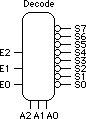
Decode -- 3-8 Decode; three address lines select one of eight low-active outputs; three additional high-active inputs serve to enable the decoder, so that any one or more of them low leaves all eight outputs high (inactive).
Pulse -- One-shot Pulse Generator. Its output
goes low for three gate delays shortly after the rising edge of its input,
then goes high and stays there until the next low-to-high transition of
its input. Use this to generate a short pulse for writing to RAM or latching
flip-flops.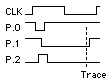 A second output is stretched to be synchronized with the next trace line
if your trace is too infrequent to capture the pulse. A third output is
high-active, as required for the FF flip-flop above.
For example, the following line produces the outputs shown:
A second output is stretched to be synchronized with the next trace line
if your trace is too infrequent to capture the pulse. A third output is
high-active, as required for the FF flip-flop above.
For example, the following line produces the outputs shown:
P Pulse CLK
Renum -- Signal Renumber. This macro has no active parts,
it simply serves to rename with a sequential numbering scheme up to 32
random signals. For example:
X Renum d c b e f ais equivalent to the following six lines:
X.0 = dYou can use this macro in connection with the following signal naming abbreviations to make large circuits easier to manage. In any long stretch of inputs to a gate or memory or macro, sequentially numbered signal names can be automatically replicated by a single "+" (or "-" or "~") which is taken to mean "the same signal name, but with the sequence number after the dot incremented (or decremented or kept the same)." For example, an 8-bit RAM with five address bits can be encoded thus (recall from the definition above that address bits are "Big-Endian" while data bits are "Little-Endian", referring to which end of the sequence starts first):
X.1 = c
X.2 = b
X.3 = e
X.4 = f
X.5 = a
Sample RAM 8 A.4 - - - - Wr D.0 + + + + + + +The above line is exactly equivalent to the following line (but somewhat easier to type and read):
Sample RAM 8 A.4 A.3 A.2 A.1 A.0 Wr D.0 D.1 D.2 D.3 D.4 D.5 D.6 D.7Note that the number must be at the end of its name, and the dot is required to separate it from the rest of the name.
Another abbreviation replicates sequentially numbered lines. In the first of the following two lines, every asterisk is replaced by the number at the front of the following line, and counted down to zero; the singleton asterisk on the second line triggers the replication. Thus these two lines:
Sig.* gate enb P* R.*.0are exactly the same as (that is, in processing are placed by) these five lines:
4 *
Sig.4 gate enb P4 R.4.0Note that the star can occur anywhere and any number of times in the line being replicated, but it always counts down to 0 equally for every occurance. These two forms of replication can be combined as needed. The Renum macro makes it easier to build sequential numbers on arbitrary signal names, for use with these abbreviations.
Sig.3 gate enb P3 R.3.0
Sig.2 gate enb P2 R.2.0
Sig.1 gate enb P1 R.1.0
Sig.0 gate enb P0 R.0.0
Rev. 2003 November 17